1 Introduction
Electromagnetic forming is a high-speed forming process which operates on an energy-based principle and thus offers contactless force transmission. It is typically applied for the forming of sheets with thicknesses larger than 1 mm [1] and is also used to process metal tubes [2]. Besides forming [3] it is also applied for operations like cutting [4], joining [5] and embossing [6]. Further advantages which bring this process in the focus of investigations are a one-sided die [7], high strain rates [8] with following changes in plastic material properties of the workpiece [9]. Furthermore, the workpiece behavior exhibits less wrinkling [10] and springback [11] due to this forming process.
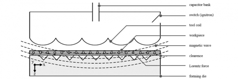
The energy for the electromagnetic forming is provided by a capacitor bank. A high sinusoidal discharge current is generated by short-circuiting the capacitor bank and is conducted through a tool coil. Thereby an electromagnetic field is produced which in turn generates an eddy current in the electrical conductive workpiece. Due to the field of the tool coil and the eddy current in the sheet, a repulsive force (Lorentz force) pointing away from the tool coil is generated. Depending on the workpiece thickness, the resulting Lorentz forces can act as body forces that accelerate the workpiece onto the forming die (see Fig. 1). In the case of thin sheets, the penetration depth of the electromagnetic field is larger than the sheet thickness (skin depth > sheet thickness) and the body force acts in the complete workpiece volume. In terms of process efficiency, however, the degree of effectiveness is reduced. For compensation, driver sheets positioned between tool coil and workpiece are applied to accelerate the workpiece [12]. Another strategy to increase process efficiency is incremental forming by multiple discharges of the tool coil [13].
Fig. 1: Principle of electromagnetic forming with an embossing die
The potentials of electromagnetic forming are sufficiently known in the field of macro forming, i.e. in the range of sheet thicknesses above 1 mm [14]. Here, however, forming, joining, and cutting operations are the focus of attention. The aim for the embossing of structures is to generate high impact pressures with a flight phase before die contact [15]. The transfer of this effect to the embossing of thin sheets was shown by Langstädtler et al. [16]. Moreover, they also investigated the influence of the workpiece thickness and the use of driver sheets in electromagnetic embossing of microstructures. It could be demonstrated that by increasing the distance between the die and workpiece an improved embossing result can be achieved and that driver sheets are a suitable process variant. Langstädtler et al. also identified the rebound effect and air drag as a challenge from the electromagnetic embossing of microstructures.
Kamal et al. [6] investigated electromagnetic embossing of microstructures in two stages. They identified further problems regarding significant die wear and sheet metal-die welding and concluded that die materials as well as coatings should be investigated to minimize these phenomena. Herrmann et al. [17] examined DLC-coated dies for embossing of aluminum sheets and reduced the adhesion significant compared to dies out of aluminum, copper and two tool steels.
In this study, the embossing of pyramidal structures in the micro scale with an aspect ratio of about 1 into thin aluminum sheets is investigated. Due to the pyramidal geometry, this type of structures poses specific challenges on the replication fidelity to reproduce the sharp edges and corners on the sheet metal. The structures used for the experiments in this work were generated by Diamond Micro Chiseling (DMC), a dedicated process for manufacturing a variety of prismatic features in optical quality on a micro scale [18]. Typical applications of DMC include the generation of retroreflective surfaces with full cube corner geometry [19, 20]. The reproduction of the microstructure is assessed by a lateral analysis and an indirect determination of the structure height, resulting from its geometric specifications. In addition, the changing surface roughness of the sheets by impulse forming is considered from relatively rough initial surfaces with a rolled texture to smoother embossed surfaces. Finally, this study reveals basic approaches and process variants to replicate optical microstructures by electromagnetic embossing.
2 Experimental setup
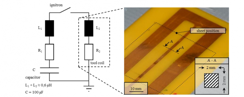
A capacitor bank with a maximum charge energy of 1800 J, which can be actuated by a single ignitron (National Electronics NL508/NL508A), is used for all forming experiments. The inductance (see Fig. 2) of the components results in a discharge frequency of ~14.5 kHz, which results in a calculated penetration depth (1) of 678 µm in aluminum according to Psyk et al. [21]:
A three-bar coil, consisting of copper (2.0060 / E-Cu57) with a minimum cross-section of 2 x 2 mm² in the forming area, is used as tool coil. The distance between tool coil and workpiece is 195 µm, with polyimide foil as insulation. All experiments are performed without clearance between workpiece and die. The outer return bars of the three-bar tool coil are broader and not used for forming.
Fig. 2: Setup of the tool coil
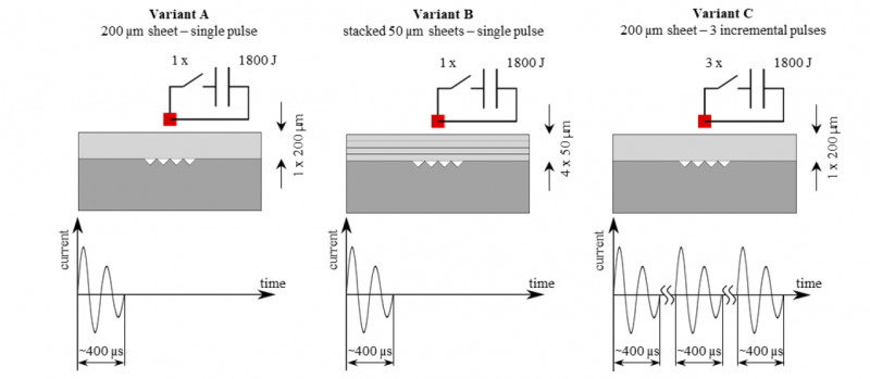
To replicate the microstructured die three different process variants are investigated (see Fig. 3). Variant A is the conventional embossing setup with a 200 µm sheet and without clearance and one single pulse. Variant B is the partitioning of the workpiece in four individual 50 µm sheets, so the three top layers act as driver sheets, treated with one single pulse. The last setup, Variant C, is based on the first setup, but the 200 µm sheet was treated with three incremental pulses with the capacitor completely discharged in between without moving the sheets intermediately. Aluminum sheets (3.0255 / Al99,5) with a size of 50 mm by 50 mm in two thicknesses (50 µm and 200 µm) are used as workpiece or driver sheets. The surface roughness is determined by a white light interferometer (WLI) (Taylor Hobson CCI HD). A scanning electron microscope (SEM) was used to image surfaces on sheets and the die and to perform energy dispersive X-ray spectroscopy (EDX) and backscattering electron (BSE) analyses.
Fig. 3: Process variants (methods and current pulses), single pulse with 200 µm sheet (Variant A), single pulse with four stacked 50 µm sheets (Variant B) and three incremental pulses with 200 µm sheet (Variant C)
The retroreflective array was machined by Diamond Micro Chiseling on a base body, which is made of nickel silver N37 (2.0790 / CuNi18Zn19Pb1). This material allows for the generation of a large number of pyramidal structures without significant tool wear and thus was used for the retroreflective array in this study [22]. The array consists of 238 interlaced pyramidal structures with a structure angle to the base surface of 54.74°. As shown in Figure 4, the die consists of three-sided pyramids arranged in a hexagonal pattern with a lateral pitch of 150 µm from peak to peak. The resulting total structure height (peak to valley in z-direction) is 122.5 µm, which leads to an aspect ratio of 0.82. The total lateral area of the diamond micro chiseled array amounts to 2.3 x 2.3 mm².
Fig. 4: Scanning electron microscope (SE-sensor) images of the die before usage at different magnification levels
3 Results
3.1 Workpiece related results
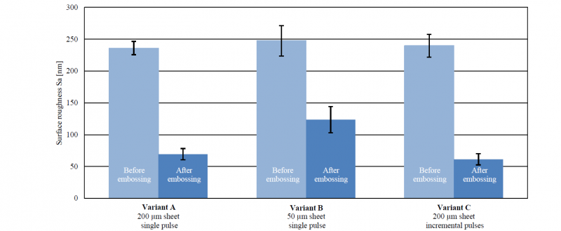
In the context of electromagnetic embossing of microstructures, the question emerges regarding the required initial roughness of the sheets in order to properly emboss optical features. For this purpose, the roughness of the die-sided faces of the sheets before and after embossing was determined (see Fig. 5). For Variant B, only the bottom sheet facing the die was evaluated. Due to the steep structure angles of the facets in combination with their optical surface quality (causing multiple reflections), it was not possible to measure the roughness directly on the pyramidal structures with the optical WLI microscope. Instead, the roughness that was formed on the surrounding optical plane surface of the die was observed. It can be seen that the roughness of the sheets is reduced, however, they are still not in the optical range (Sa ≤ 10 nm). It can be assumed that when the embossing energy is increased, the achievable roughness will be further reduced.
Fig. 5: Surface roughness Sa of metal sheets before and after electromagnetic embossing, error bars indicate standard deviation with n = 10 (Variant A + B) and n = 5 (Variant C)
As the facets of the pyramidal structures visually appear homogeneous and with few distortions in the in the SEM images (see Fig. 6), it can be assumed that the surface roughness on the facets is lower than the surface roughness of the plane surface next to the array. This can be explained by the higher contact pressure that acts in the area of the array. Only a fraction of the total surface has contact with the die wherever the pyramidal structures are formed. On the examined surrounding plane surface, the sheet has contact with the die over the entire surface. In conclusion, this means that the roughness of the sheets can also become optical in the area of the plane surface as soon as enough charge energy is available for electromagnetic embossing.
During the experiments multiple embossed structures were found on all processed sheets (see Fig. 6). These are caused by the sheets bouncing onto the die repeatedly and shifting laterally between the impacts. In the fringe region of the embossed array the multiple embossed structures can be observed more frequently. The reason for this is due to the presence of a plane surface next to the array, which is in one level with the structure peaks of the array. The flat surface supports the sheets and promotes a bouncing effect between sheet and die. Furthermore, the incremental embossing of the sheet shows a much higher number of multiple embossed structures in the fringe region. This is related to the repeated excitation of the sheet by the tool coil.
However, it is still not understood on what the described bounce effect is based. On the one hand, it could be a mechanical bounce caused by the initial impact of the sheet metal. On the other hand the bounce effect could be caused by the sinusoidal discharge of the tool coil. All multiple embossed structures show a direction, which is caused by the delayed impact of the sheet on the die. It is noticeable that the directions within a sheet vary, which excludes a simple linear shift of the entire sheet. When evaluating the different directions within a sheet, it is concluded that the sheet cannot be simply rotated during the embossing process either. Rather, two possible explanations for the different embossing directions can be summarized: 1.) There are time-delayed mechanical bouncing effects that spread out in waves and thus influence each other and lead to a complex arrangement of the embossing directions. 2.) The induced tangential forces caused by the induced current in the sheet and the interaction with the magnetic field lead to lateral partially different (elastic) stretching and compression of the sheet, which thus impacts the die at different points in time.
Fig. 6: Scanning electron microscope (SE-sensor) images of multiple embossed structures, 200 µm sheet – single pulse (Variant A), stacked 50 µm sheets – single pulse (Variant B) and 200 µm sheet – 3 incremental pulses (Variant C)
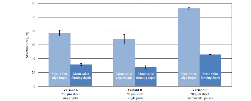
Figure 7 shows the maximum achieved structure sizes on the die-sided sheets and corresponding forming depths of the die penetrating the sheets including mean values from five values per embossed sheet. Figure 8 shows the largest embossed structures observed on the processed sheets. The incremental embossing process (Variant C) produces the largest embossed structures with a maximum edge length of 114 µm, which corresponds to a forming depth of 46.6 µm while the nominal height of the die measures 122.5 µm. The mean value of the five largest embossed structures is 112.6 µm edge length, representing a forming depth of 46 µm. For the sheets embossed in the single pulse process with stacked 50 µm sheets (Variant B), smaller structures are obtained. The largest pyramidal structure detected on one of two 50 µm sheets has an edge length of 76 µm, which corresponds to a forming depth of 31 µm. On the second 50 µm sheet the maximum edge length is 64 µm. The mean value of the five largest structures on the two sheets is 68.2 µm. In comparison, larger structures were generated on the 200 µm sheets using the same embossing strategy (Variant A). The maximum edge length detected amounts to 83 µm, which corresponds to a forming depth of 33.9 µm. The maximum structure edge length on the second sheet is 74 µm. The mean value of the five largest structures on two 200 µm sheets is 77.1 µm.
It is apparent that the four stacked 50 µm sheets (Variant B) produce smaller structure sizes than the 200 µm sheets (Variant A). This can be explained by three factors. First, even if the total sheet thickness is the same for both variants, the induced current flows are not identical. In the stacked sheets there are four separate smaller current flows due to the contact resistance between the sheets because of oxide layers and small roughness induced gaps, whereas in the 200 µm sheet a large current flow is induced. This can lead to the effect that the force applied to accelerate the sheets onto the forming die is different for the two process variants. The second factor takes into account that the force decreases due to the higher number of interfaces where the pressure wave passing through the sheets is reflected. The third factor is the elastic recovery at the roughness peaks of the 50 µm sheets, which removes energy from the embossing process and thus leads to smaller forming depths.
Fig. 7: Embossed structure sizes for different embossing strategies, error bars indicate standard deviation with n = 10 (Variant A + B) and n = 5 (Variant C)
The incremental embossing process with its three pulses introduces more energy into the forming process, resulting in the largest structure sizes. Compared to the single pulse variants, multiple embossed structures occur more frequently in the fringe region and less frequently in the center of the embossed array. A possible explanation for this is that the already embossed structures from the preceding pulses act as guiding structures, holding the center of the array in place for subsequent pulses. In contrast, multiple embossed structures occur in the fringe region as plane surface next to the array provides no guidance here.
Fig. 8: Scanning electron microscope (SE-sensor) images of the largest structures achieved for each embossing strategy, 200 µm sheet – single pulse (Variant A), stacked 50 µm sheets – single pulse (Variant B) and 200 µm sheet – 3 incremental pulses (Variant C)
Depending on the embossing variant, the material flow originates either from the thickness or from the width of the sheet. An examination of the back of the sheet may be used to indicate the predominant mechanism in this case. If it is a flow in the sheet thickness, the backside of the sheet should not have changed. Thus, there should be no visible change in the back of the sheet induced by the forming process. If, however, material flows in the sheet width, the backside should be ideally an exact negative copy of the formed front side of the sheet, i.e. the positive geometry of the die. Figure 9 shows the backsides of a 50 µm sheet (die related sheet from four stacked 50 µm sheets) and a 200 µm sheet, both of them formed in the single pulse process. The new die is additionally shown for comparison on the left.
Fig. 9: Scanning electron microscope (SE-sensor) images of a) the die before usage, b) the backside of an embossed 200 µm sheet (Variant A) and c) the backside of a die-sided embossed 50 µm sheet (Variant B)
On both back sides of the sheets a deformation can be observed. On the 50 µm sheet, the structures of the die can be seen indistinctly, whereas on the 200 µm sheet only a square bulge is visible. This indicates that each of these forming processes are hybrid variants. In principle, the thicker the sheet, the higher the proportion of material flow from the sheet thickness.
3.2 Die related results
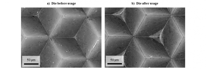
The embossing die was used in a total of seven embossing operations. It was examined with a scanning electron microscope before and after usage (see Fig. 10). Apart from slight deformations at the structure peaks and edges, there is no geometrical change of the die. Comparing the images before and after using, it is noticeable that a change at the structure peaks appeared. SEM-EDX and SEMBSE analysis have shown that the bright area is not aluminum adhesion, but indicate that the brighter areas contain less oxygen and carbon. The oxygen suggests an oxide layer on the surface might have been removed by the impacting sheets. The carbon can indicate contaminations in the darker areas. In the brighter areas at the structure peaks, these contaminations may have been removed by impacting sheets during embossing.
Fig. 10: Scanning electron microscope (SE-sensor) images of the die a) before usage and b) after seven electromagnetic embossing operations
Apart from the intact pyramidal structures described above, areas of mechanical damage to the structure peaks appeared on the die. Figure 11 shows the most significant damage found. About one third of all structure peaks show such damage in similar or reduced form. Since all damage points in the same direction and are not arranged randomly like the multiple embossed structures, it is assumed that the damage does not result from the electromagnetic embossing process itself, but from handling, e.g. when detaching the sheet manually from the die after embossing. It can be excluded that the damage occurred during cleaning of the die, since it was only rinsed with isopropanol without mechanical contact before and between the experiments.
Fig. 11: Scanning electron microscope (SE-sensor) images of mechanical wear at the structure peaks after seven electromagnetic embossing operations
4 Conclusion
In this work, highly complex optical microstructures were partially embossed into thin aluminum sheets by means of electromagnetic embossing. For this purpose, different process variants and sheet thicknesses were applied. The following major points can be concluded:
-
Electromagnetic embossing significantly reduces sheet roughness, i.e. it is not necessary to provide sheets with a roughness already in the optical range.
-
Multiple embossed structures occur particularly in the fringe region of the die.
-
Four stacked 50 µm sheets do not yield the same replication quality as a single 200 µm sheet with otherwise identical process parameters. This reflects the higher number of interfaces and the resulting change in mechanical and electrical response.
-
Incremental processing by consecutive current pulses is possible and leads to higher replication quality.
-
The electromagnetic embossing of thin sheets is a mixture of material flow from the sheet width and the sheet thickness.
-
The optical highly complex structures of the die largely withstand the stresses of seven embossing operations; slight deformations occur at the structure peaks of the die.
Consequently, it has been shown that electromagnetic embossing is a promising approach for the replication of optical microstructures in thin metal sheets. In the future, the origin and, thus, prevention of multiple embossing should be investigated more closely. A possible method is the adjustment of the capacitor discharge regarding a single Lorentz force impact. Moreover, the investigations regarding die wear should also be intensified.
Acknowledgements
The authors would like to thank the German Research Foundation (DFG - Deutsche Forschungsgemeinschaft) for funding this work within the project: “Electromagnetic Embossing of Optical Microstructures” (Grant numbers: BR 825/79-1 and KU 1389/17-1).
